Name:_____________________________
Please fill out this lab and hand it in with the required printouts attached. This lab is due in one week. Label your attachments (Problem 1, Problem 2, etc., and put them in order).
LogicWorks Laboratory One
Introduction to Windows/Macintosh(TM) and LogicWorks
Objectives
This lab will introduce you to LogicWorks. After completing this assignment, you should understand how to draw circuit schematics and simulate simple combinational circuits.
If you are unfamiliar with the Windows/Macintosh interface, find a fellow student who is familiar with it and work with that person for this first assignment. If you are familiar with the interface, please help out fellow students who might not be.
For each lab you will need to hand in the summary sheet (the last page of this and future assignments) and any hardcopy requested (indicated in the text by a bullet symbol).
Please type all of your (attached) written work. Spelling and mechanics count! You may fill out the tables by hand...any drawings must be attached.
A Note about LogicWorks at UB
About the DOS installation:
If there is no logic directory on the c drive then...
Install logic works, type the following at the dos prompt:
md C:
xcopy f:.* C:
noemm
<reboot, ie. alt-ctrl-del>
cd logic
logic
To Print:
Use the PC with the dot matrix printer. Then issue the print command.
If you have a problem, see Zahid.
Half-Adder Circuit
The half-adder is a function that takes two inputs, X and Y, and produces two outputs, SUM and CARRY. Fill in the truth table for the behavior of the half-adder:
  X       Y     Sum   Carry
  0       0
  0       1
  1       0
  1       1
Draw a schematic for the half-adder in the space above. Use only NOT, AND, and OR gates.
Full-adder Circuit
Repeat Problem 1 for the full-adder circuit, which takes three inputs and produces the two outputs SUM and CARRY. Draw the full-adder in the space provided. Use only NOT, AND, and OR gates.
  X       Y      Z     Sum   Carry
  0       0      0
  0       0      1
  0       1      0
  0       1      1
  1       0      0
  1       0      1
  1       1      0
  1       1      1
Using LogicWorks
In this section, you will use LogicWorks to enter the schematic for the half-adder. LogicWorks is a tool for entering gate level schematics of a digital system and performing simulations of its behavior.
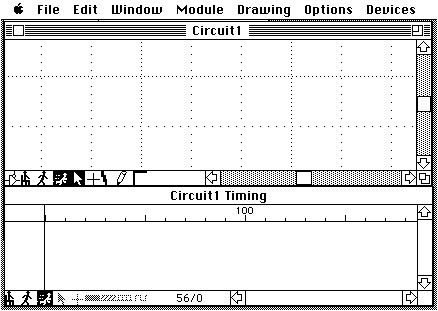
Double-clicking on the LogicWorks icon results in the following screen:
The Circuits window is used for drawing schematics, and the lower Timing window displays waveforms of instrumented "nodes" (that is, the labeled wires) within the schematic, similar to an oscilloscope trace. We are now ready to enter gate schematics.
Creating Simple Circuits
Let's start with a very simple circuit: an AND gate. Make sure that the Circuit window is selected (it will appear highlighted as in the screen image above). Click on the Devices menu.
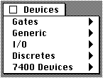
It should look something like the menu above. The devices available to you are grouped into five classes or libraries: gates, generic, I/O, discretes, and 7400 series TTL as shown in the menu above. These are the standard default libraries. Gates are the standard simple logic gates, such as AND, OR, and NOT. Generic devices include more complex building blocks, which we will not be using in this lab. I/O includes switches, keyboards, and probes. Discrete devices consist of electrical components, such as power supply connections, batteries, etc. With the possible exception of +5V and ground, we will not be using these very much. The 7400 series is a collection of frequently used TTL components. In fact, these choices of devices are only what is available by default. It is possible to create libraries of additional devices (the 7400 series devices are included this way; they are not really built into LogicWorks) or to create certain kinds of devices on the fly, which we will see in later labs. The (partial) contents of the device menus are shown below. The little arrow at the bottom of the menu means that there are more choices.
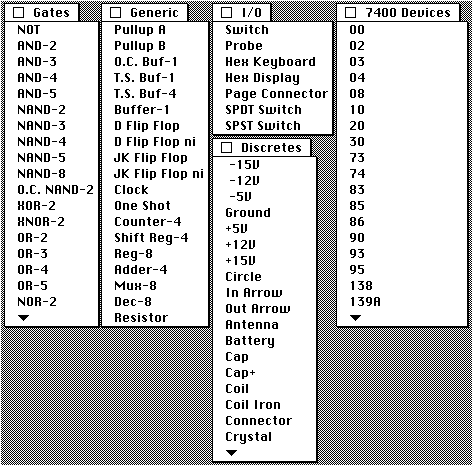 Select a
two-input AND gate (point the mouse at the word Libraries in
the title bar, press the mouse button, and while holding it down,
drag the mouse down to select the word Gates). The
Gates submenu pops up. With the mouse button still held down,
select AND-2 (it should be in "inverse%20video" if you did the right
thing ). Now let up on the mouse button. Move the pointer to the
middle of the Circuit window. Note that the pointer turns into an
image of the AND gate. Press down on the mouse button to place the
AND gate in the circuit window.
Select a
two-input AND gate (point the mouse at the word Libraries in
the title bar, press the mouse button, and while holding it down,
drag the mouse down to select the word Gates). The
Gates submenu pops up. With the mouse button still held down,
select AND-2 (it should be in "inverse%20video" if you did the right
thing ). Now let up on the mouse button. Move the pointer to the
middle of the Circuit window. Note that the pointer turns into an
image of the AND gate. Press down on the mouse button to place the
AND gate in the circuit window.
Note that the gate menu provides NOT, AND, and OR gates, the latter with from two to five inputs. For the moment, we will not be using the other available gates.
An AND gate by itself is not very interesting. So let's wire it up with some input switches and an output probe. These can be selected from the Libraries menu and its I/O submenu. Select the probe in the same manner that you selected the AND gate: pull down the Libraries menu, drag to the I/O submenu and then the probe selection. Let up on the mouse button to select the probe. Now move the pointer into the Circuit window. Once again, it turns into a rectangular icon, representing a probe. Position the probe so that its connection wire coincides with the output wire of the AND gate (this is sometimes called "wiring by abutment" ). Click the mouse to place the probe. The wires will "flash" to indicate that the connection has been made. The probe will "read-out" an X: this means that the output is undefined so far, because we have not connected any inputs to the AND gate.
Repeat the process to select a switch from the Libraries menu/I/O submenu. Place one switch near the top input to the AND gate (remember, you place by clicking the mouse button), reposition to a spot near the bottom input, and hit the mouse button to place the second switch. At the moment, the switches are not yet connected to the AND gate. To place yourself in "wiring" mode, select POINT from the Edit menu, or click on the pointer shown at the lower left of the Circuit window, or hit the space bar. The pointer turns back into the familiar arrow. Now use it to point at the tip of the AND gate's top input. With the mouse button down, drag the mouse, and you will see a wire segment extend from the input. Pull it toward the switch. You can create additional segments by letting up on the mouse, clicking on the end of the last segment, and with the button still down, dragging up or down in the direction you want to go. Note that just because two wires cross, it does not mean that are connected! You must explicitly drag one segment to a point on the other and let up on the mouse button to cause the connection to be made. The wires should "flash" to signal that the connection has taken place. You can check on the connectivity of a series of wire segments by clicking on a segment of the wire while in the pointer mode. All connected segments will be highlighted. It is a good idea to check your connections, because wires that appear to be connected might actually be independent wires merely close together. Also observe that all the device pins connected to the wire are highlighted. Sometimes a wire will appear to be connected to a device pin when it isn't. Selecting the wire will show if this is the case. Using the wiring procedure just described, wire up the switches to the AND's inputs. If the connections have been made correctly, the probe should change its read-out from X to 0 (assuming that the switches are still set to zeros).
If you have made a mistake in the wiring, you can fix it by entering the ZAP mode, which can be selected from the Edit menu or by clicking on the lightning bolt on the lower left of the Circuit window. This turns the pointer into a lightning bolt. Simply point the tip of the lightning bolt at a wire segment or a gate, click, and the object will disappear. Be careful in how you use this! It is quite easy to zap the wrong thing, and this operation cannot be undone.
To change the switch settings, click the mouse in the middle of the switch. This will cause it to toggle from a 0 to a 1 or vice versa. Try all of the possible switch settings of the two inputs to convince yourself that the gate actually behaves like an AND gate!
There is one more mode we haven't told you about yet: the NAME mode, also available under the Edit menu or by clicking on the pencil on the Circuit window. Select it and you will discover that the pointer turns into a pencil. It is used for placing names on nodes within your circuit for later use with the Timing window. Label the input switches A and B, and the output Z, by placing the tip of the pencil on a wire segment and clicking the mouse. The pencil changes to an I-bar, denoting text input. Type your label name and hit the return or enter key. Two things happen: (1) the pointer turns back into a pencil, and (2) the name you just typed appears in the Timing window. Try toggling the switches a few times. Note how a timing waveform is drawn out across the screen.
(NOTE: Make sure that the label is attached to the wire. This is a common source of headaches. The label may have attached itself to another nearby wire or gate pin or it may be even completely unattached if you did not click the pencil close enough to the wire. The signal name will only appear in the Timing window if it is attached to a wire. You can check for this by getting out of the NAME mode - by hitting the space bar as a shortcut or selecting the arrow cursor at the bottom of the window - and then selecting the signal name or wire. You select by clicking on it when the cursor is arrow-shaped. If the two are attached, then selecting one will cause both to be highlighted. If they are not attached then only the one you directly selected will be highlighted. If this occurs, delete the label and try it again while being more careful to position precisely the pencil point when you click.)
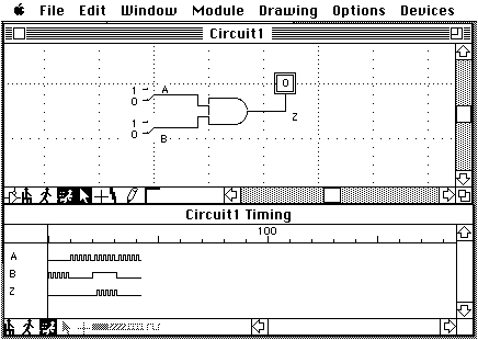
Here is a sample of what you should be seeing on your screen right now:
To save your work, simply use the SAVE CIRCUIT AS command under the File menu.
Experimenting with the Half-adder
Enter into LogicWorks the schematic you developed for the half-adder. Label the two inputs as X and Y, and the outputs as SUM and CARRY. Use switches at the inputs and probes at the output. Convince yourself that the schematic actually does perform the function of the half-adder by cycling through the four input combinations of the inputs and checking that the probe readings match your expected results.
(NOTE: To run a simulation, make sure that the little man with the hat is walking or running - see the mode bar at the bottom of the window. If he is sitting down then the simulator is in "single-step" mode, and it will appear as if nothing is happening. Single-step mode is used when you want the simulation to proceed under your control. You can advance the simulation to the next event - transition on a wire - by clicking on the figure of the little man sitting. The walking and running figures are used to set the simulator to run at slow or fast speeds. You should set the little man to one of these two modes.)
1. When you have completed the working circuit, print a copy of the circuit and the Timing window showing that it works correctly.
The Full-Adder
Now enter the schematic for a full-adder and verify its operation using simulation.
2. Print the circuit and the timing diagram of the simulation verifying its operation.
Waveforms as Inputs
The Timing window shows the behavior of the circuit as a function of time. Every time we click on an input switch, the simulator that underlies LogicWorks determines that a new event has taken place. It propagates this event through its model of the schematic's behavior and timing, until the output values change. Unless you specify otherwise, LogicWorks assumes that all gates take a single unit of delay. If you look closely at the timing waveforms, you will discover that the output changes lag behind the input changes. The LogicWorks manual explains how to change the resolution of the timing waveforms (see TIMING OPTIONS under the Options menu). Simulate the half-adder circuit, looking closely at The timing window to see how the changes propagate through the circuit.
Besides using switches as a source of inputs, you can also draw your own input waveforms and then apply them to the schematic in the Circuit window. First clear the Timing window by selecting CLEAR TIMING under the Options menu. Because LogicWorks reacts to every input change you make as soon as you make it, it is a good idea to pause the simulation while you enter multiple waveforms. This is done by selecting SINGLE STEP under the Options menu, or by clicking on the icon of the little man sitting on a chair. Now click in the Timing window to select it. It will become highlighted. To associate a waveform with a signal, click on the plus sign icon at the bottom of the Timing window. The cursor turns into an X. Position it at the right of the signal name, and click and drag the mouse. Starting near the lower right-hand edge of the signal name gives you a logic 0, and clicking near the upper right-hand edge yields a logic 1 waveform. You insert transitions by using the icon that looks like a square wave. After clicking on this, the cursor looks like a falling signal edge. Click on the wave form with this tool, and a transition is inserted. The current location of the cursor in the time domain (the X axis of the Timing window) is displayed at the bottom of the window, so you can very accurately insert your transitions. Then go back and change the cursor back into an X, click on the waveform segment you wish to change, and drag it up or down. Although you can undo your last waveform edit if you don't get quite what you wanted, you may need to CLEAR TIMING and start drawing the waveform from scratch, so be careful as you enter them.
Enter waveforms for X and Y that exercise all four of the possible input combinations. Note that you cannot use the waveform editing tools unless the little man is sitting! Spread the waveforms out across the screen. Here is what it should look like:
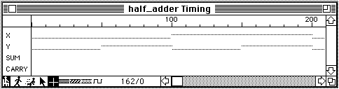
The dotted lines represent the waveform as it will be applied to circuit, starting at the left and advancing to the right. Transitions have been placed at time points 50, 100, 150, and 200.
Now click on the walking or running little man (or select WALK or RUN from the Options menu). You should see something that looks like this in the Timing window:
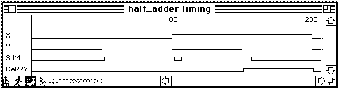
Now the dotted lines have been replaced with solid lines, and waveforms appear for the outputs. If you watch carefully, you can even see your switches change in response to the transitions in the timing waveforms. Note the glitch (also called a hazard) in the SUM waveform. You probably didn't notice this behavior when entering the inputs with the switches, but it happens even there. (Try it: simulate with the switches set for X = 0 and Y = 1, place the simulation in single step, change the switches to X = 1 and Y = 0, then click on the sitting man a few times, while keeping a close eye on the SUM probe. You should see the probe very briefly register a 0!). This behavior is intrinsic to the implementation of the half-adder.
3. Did you obtain a comparable waveform? If it differed, explain why it did. (HINT: it is highly unlikely that the waveform you see on your screen is exactly the same as the one included here!). Using pencil and paper, trace the flow of signals through your half-adder schematic for the X: 0 => 1, Y: 1 => 0 transition. Use this to explain why the glitch took place.
Adding Delay
By default, all gates in LogicWorks have unit delay. This is not particularly accurate. Glitch behavior can be made more obvious by associating more accurate delays with the gates of your schematic. This is done by selecting a gate in the schematic (be in POINT mode and click on the gate), and then selecting SET PARAMS from the Options menu (you can also do this by holding down the option-key while clicking on the gate). The ensuing dialogue allows you to change the input-to-output delay for that particular (Click here for a demo!) gate:
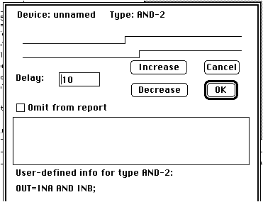
The animation shows how to set the input delay for an inverter...but you can use any gate you like....even custom gates. So you do not have to do this for this particular lab...This is only for your information....
You should choose your implementation to reduce the number of chips you will have to use. Please do not just copy a full-adder circuit from the text--we will expect you to explain your circuit on demand! After you decide on a design, use LogicWorks to build a schematic using devices from the 7400 library.
Review
In this laboratory, you should have acquired an understanding of the following concepts and skills:
o how to use a tool like LogicWorks to construct simple schematics
o how to simulate and verify the behavior of a circuit using switch inputs and timing waveforms
o the effect of delay on waveforms
LogicWorks Laboratory One
Introduction to Windows/Macintosh(TM) and LogicWorks
Summary Sheet
(Include this as the cover for what you hand in.)
Name:_____________________________
1. Hardcopy of half-adder circuit and the contents of the Timing window after simulation.
2. Hardcopy of full-adder circuit and the contents of the Timing window after simulation.
3. Hardcopy of the Timing window showing a glitch on the SUM output of the half-adder and an explanation as to why this occurs.